- 您现在的位置:买卖IC网 > Sheet目录2006 > LTC2494IUHF#TRPBF (Linear Technology)IC ADC 16BIT W/PGA 38-QFN
LTC2494
2494fd
applications inForMation
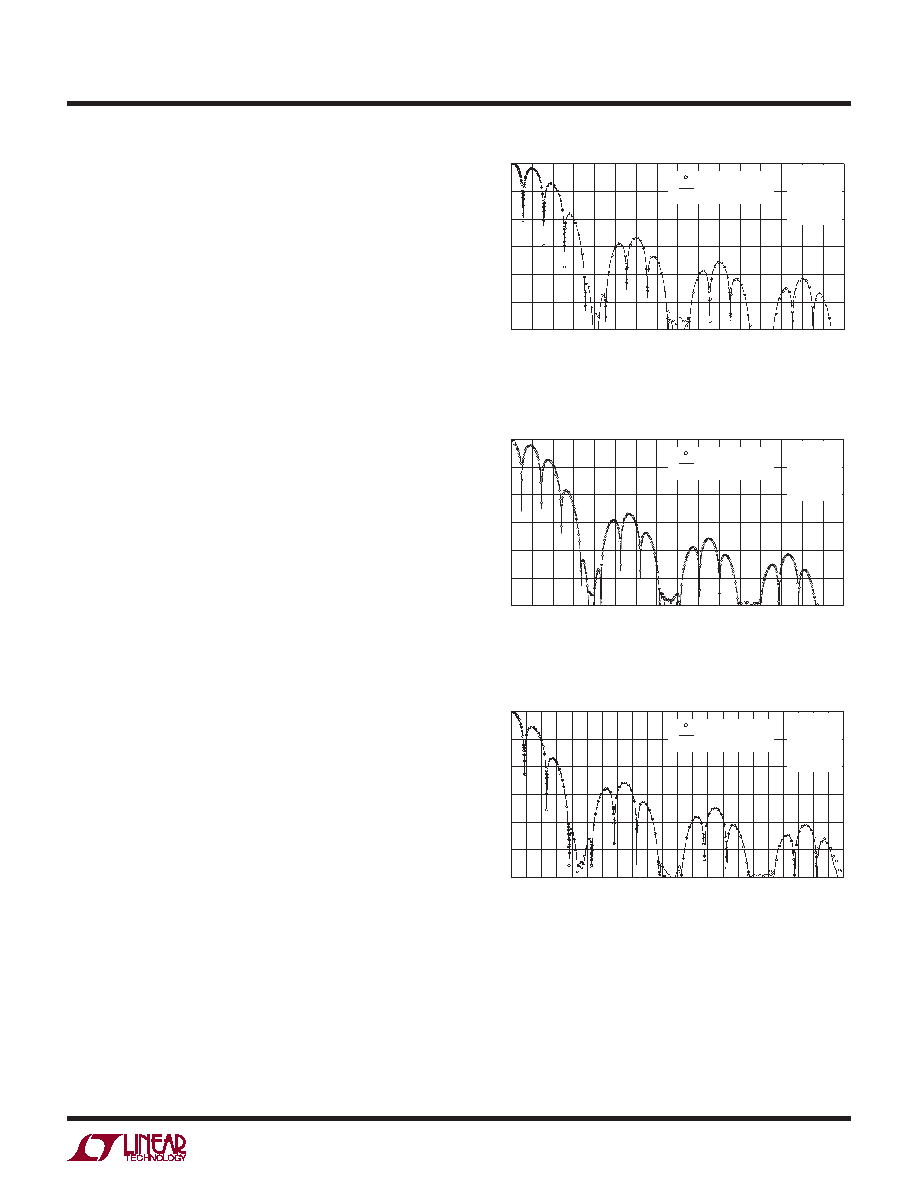
The user can expect to achieve this level of performance
using the internal oscillator, as shown in Figures 23, 24
and 25. Measured values of normal mode rejection are
shown superimposed over the theoretical values in all
three rejection modes.
Traditional high order delta-sigma modulators suffer
from potential instabilities at large input signal levels.
The proprietary architecture used for the LTC2494 third
order modulator resolves this problem and guarantees
stability with input signals 150% of full-scale. In many
industrial applications, it is not uncommon to have mi-
crovolt level signals superimposed over unwanted volt
level error sources with several volts of peak-to-peak
noise. Figures 26 and 27 show measurement results for
the rejection of a 7.5V peak-to-peak noise source (150%
of full-scale) applied to the LTC2494. From these curves,
it is shown that the rejection performance is maintained
even in extremely noisy environments.
Using the 2x speed mode of the LTC2494 alters the rejec-
tion characteristics around DC and multiples of fS. The
device bypasses the offset calibration in order to increase
the output rate. The resulting rejection plots are shown
in Figures 28 and 29. 1x type frequency rejection can be
achieved using the 2x mode by performing a running
average of the conversion results (see Figure 30).
Output Data Rate
Whenusingitsinternaloscillator,theLTC2494producesup
to 15 samples per second (sps) with a notch frequency of
60Hz. The actual output data rate depends upon the length
of the sleep and data output cycles which are controlled
by the user and can be made insignificantly short. When
operating with an external conversion clock (fO connected
to an external oscillator), the LTC2494 output data rate
can be increased. The duration of the conversion cycle is
41036/fEOSC. If fEOSC = 307.2kHz, the converter behaves
as if the internal oscillator is used.
AnincreaseinfEOSCoverthenominal307.2kHzwilltranslate
into a proportional increase in the maximum output data
rate (up to a maximum of 100sps). The increase in output
rate leads to degradation in offset, full-scale error, and ef-
fective resolution as well as a shift in frequency rejection.
Whenusingtheintegratedtemperaturesensor,theinternal
Figure 23. Input Normal Mode Rejection vs Input Frequency with
Input Perturbation of 100% (60Hz Notch)
Figure 24. Input Normal Mode Rejection vs Input Frequency with
Input Perturbation of 100% (50Hz Notch)
Figure 25. Input Normal Mode Rejection vs Input Frequency with
Input Perturbation of 100% (50Hz/60Hz Notch)
INPUT FREQUENCY (Hz)
0
15
30
45
60
75
90 105 120 135 150 165 180 195 210 225 240
NORMAL
MODE
REJECTION
(dB)
2494 F23
0
–20
–40
–60
–80
–100
–120
VCC = 5V
VREF = 5V
VIN(CM) = 2.5V
VIN(P-P) = 5V
TA = 25°C
MEASURED DATA
CALCULATED DATA
INPUT FREQUENCY (Hz)
0 12.5 25 37.5 50 62.5 75 87.5 100 112.5 125 137.5 150 162.5 175 187.5 200
NORMAL
MODE
REJECTION
(dB)
2494 F24
0
–20
–40
–60
–80
–100
–120
VCC = 5V
VREF = 5V
VIN(CM) = 2.5V
VIN(P-P) = 5V
TA = 25°C
MEASURED DATA
CALCULATED DATA
INPUT FREQUENCY (Hz)
0
20
40
60
80
100
120
140
160
180
200
220
NORMAL
MODE
REJECTION
(dB)
2494 F25
0
–20
–40
–60
–80
–100
–120
VCC = 5V
VREF = 5V
VIN(CM) = 2.5V
VIN(P-P) = 5V
TA = 25°C
MEASURED DATA
CALCULATED DATA
oscillator should be used (fO = 0) or an external oscillator
applied to fO, fEOSC, should be set to 307.2kHz Max.
A change in fEOSC results in a proportional change in the
internal notch position. This leads to reduced differential
mode rejection of line frequencies. The common mode
发布紧急采购,3分钟左右您将得到回复。
相关PDF资料
LTC2495CUHF#PBF
IC ADC 16BIT W/PGA 38-QFN
LTC2496IUHF#TRPBF
IC ADC 16BIT DELTA SIG 38-QFN
LTC2498IUHF#TRPBF
IC ADC 24BIT 16CH 38-QFN
LTC2600IUFD#PBF
IC DAC OCTAL R-R 16BIT 20-QFN
LTC2602IMS8#TRPBF
IC DAC 16BIT DUAL R-R VOUT 8MSOP
LTC2604IGN-1#TRPBF
IC DAC 16BIT QUAD R-R OUT 16SSOP
LTC2605IGN-1#TRPBF
IC DAC 16BIT OCT I2C 16-SSOP
LTC2606IDD#TRPBF
IC DAC 16BIT I2C V-OUT 10-DFN
相关代理商/技术参数
LTC2495CUHF
制造商:Linear Technology 功能描述:ADC Single Delta-Sigma 15sps 16-bit Serial 38-Pin QFN EP
LTC2495CUHF#PBF
功能描述:IC ADC 16BIT W/PGA 38-QFN RoHS:是 类别:集成电路 (IC) >> 数据采集 - 模数转换器 系列:- 标准包装:1,000 系列:- 位数:16 采样率(每秒):45k 数据接口:串行 转换器数目:2 功率耗散(最大):315mW 电压电源:模拟和数字 工作温度:0°C ~ 70°C 安装类型:表面贴装 封装/外壳:28-SOIC(0.295",7.50mm 宽) 供应商设备封装:28-SOIC W 包装:带卷 (TR) 输入数目和类型:2 个单端,单极
LTC2495CUHF#TRPBF
功能描述:IC ADC 16BIT W/PGA 38-QFN RoHS:是 类别:集成电路 (IC) >> 数据采集 - 模数转换器 系列:- 标准包装:2,500 系列:- 位数:16 采样率(每秒):15 数据接口:MICROWIRE?,串行,SPI? 转换器数目:1 功率耗散(最大):480µW 电压电源:单电源 工作温度:-40°C ~ 85°C 安装类型:表面贴装 封装/外壳:38-WFQFN 裸露焊盘 供应商设备封装:38-QFN(5x7) 包装:带卷 (TR) 输入数目和类型:16 个单端,双极;8 个差分,双极 配用:DC1011A-C-ND - BOARD DELTA SIGMA ADC LTC2494
LTC2495IUHF#PBF
功能描述:IC ADC 16BIT W/PGA 38-QFN RoHS:是 类别:集成电路 (IC) >> 数据采集 - 模数转换器 系列:- 标准包装:1 系列:microPOWER™ 位数:8 采样率(每秒):1M 数据接口:串行,SPI? 转换器数目:1 功率耗散(最大):- 电压电源:模拟和数字 工作温度:-40°C ~ 125°C 安装类型:表面贴装 封装/外壳:24-VFQFN 裸露焊盘 供应商设备封装:24-VQFN 裸露焊盘(4x4) 包装:Digi-Reel® 输入数目和类型:8 个单端,单极 产品目录页面:892 (CN2011-ZH PDF) 其它名称:296-25851-6
LTC2495IUHF#TRPBF
功能描述:IC ADC 16BIT W/PGA 38-QFN RoHS:是 类别:集成电路 (IC) >> 数据采集 - 模数转换器 系列:- 标准包装:1,000 系列:- 位数:16 采样率(每秒):45k 数据接口:串行 转换器数目:2 功率耗散(最大):315mW 电压电源:模拟和数字 工作温度:0°C ~ 70°C 安装类型:表面贴装 封装/外壳:28-SOIC(0.295",7.50mm 宽) 供应商设备封装:28-SOIC W 包装:带卷 (TR) 输入数目和类型:2 个单端,单极
LTC2496CUHF#PBF
功能描述:IC ADC 16BIT DELTA SIG 38-QFN RoHS:是 类别:集成电路 (IC) >> 数据采集 - 模数转换器 系列:- 标准包装:1 系列:microPOWER™ 位数:8 采样率(每秒):1M 数据接口:串行,SPI? 转换器数目:1 功率耗散(最大):- 电压电源:模拟和数字 工作温度:-40°C ~ 125°C 安装类型:表面贴装 封装/外壳:24-VFQFN 裸露焊盘 供应商设备封装:24-VQFN 裸露焊盘(4x4) 包装:Digi-Reel® 输入数目和类型:8 个单端,单极 产品目录页面:892 (CN2011-ZH PDF) 其它名称:296-25851-6
LTC2496CUHF#TRPBF
功能描述:IC ADC 16BIT DELTA SIG 38-QFN RoHS:是 类别:集成电路 (IC) >> 数据采集 - 模数转换器 系列:- 标准包装:2,500 系列:- 位数:16 采样率(每秒):15 数据接口:MICROWIRE?,串行,SPI? 转换器数目:1 功率耗散(最大):480µW 电压电源:单电源 工作温度:-40°C ~ 85°C 安装类型:表面贴装 封装/外壳:38-WFQFN 裸露焊盘 供应商设备封装:38-QFN(5x7) 包装:带卷 (TR) 输入数目和类型:16 个单端,双极;8 个差分,双极 配用:DC1011A-C-ND - BOARD DELTA SIGMA ADC LTC2494
LTC2496IUHF#PBF
功能描述:IC ADC 16BIT DELTA SIG 38-QFN RoHS:是 类别:集成电路 (IC) >> 数据采集 - 模数转换器 系列:- 标准包装:2,500 系列:- 位数:16 采样率(每秒):15 数据接口:MICROWIRE?,串行,SPI? 转换器数目:1 功率耗散(最大):480µW 电压电源:单电源 工作温度:-40°C ~ 85°C 安装类型:表面贴装 封装/外壳:38-WFQFN 裸露焊盘 供应商设备封装:38-QFN(5x7) 包装:带卷 (TR) 输入数目和类型:16 个单端,双极;8 个差分,双极 配用:DC1011A-C-ND - BOARD DELTA SIGMA ADC LTC2494